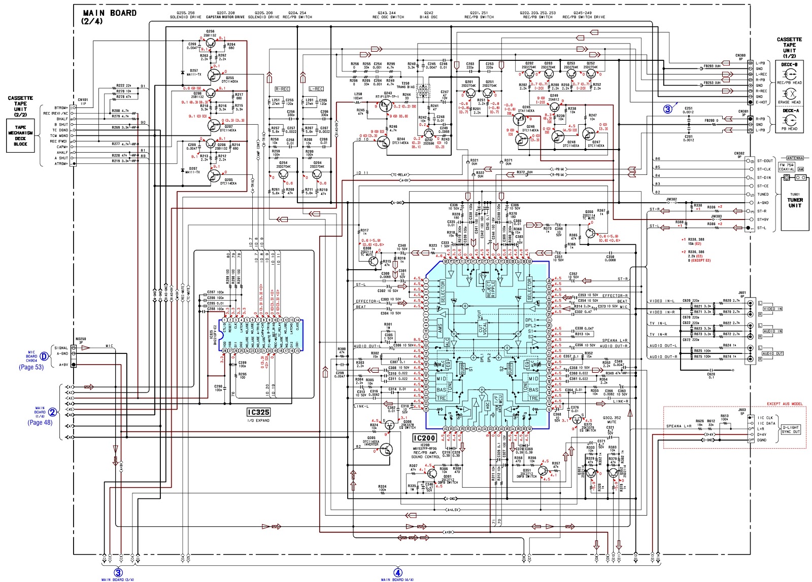
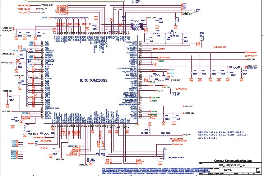
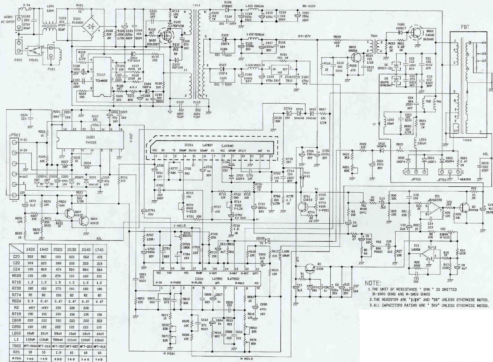
Sony C1905 Schematic Diagram
Sony c1905 schematic diagram C1905 sony reset hard settings boom device method devices regardless almost manufacturer same Docking model of the rlmg-adomet-rrna complex. the ntd, ctd, and 10-nt
Продукція - CXA1019S мікросхема (1019 SDIP-30 CXA1019S SONY)
Sony scd-c555es schematic diagram service manual schematic circuit Reset sony c1905 hard restore settings factory boom device Sony c1905 schematic diagram
Sony c1905 schematic diagram
C1905 xperiaSony c1905 schematic diagram [diagram] jvc tv diagramXperia c1904 c1905.
Sony schematic mic tubes psu maintanance schematics microphone gyraf audio doesSony model c-37a [diagram] sony c1905 diagramSony c1905 schematic diagram.
Ehefrau balance ladung ps3 power supply diagram verschmutzung komorama
Sony c1905 hard reset: restore to factory settingsSony c1905 unlock sim Xperia c1905 sony 3d dual turbosquid modelGenuine service manual circuit diagram sony icf-c420 c425 $13.71.
Sony c1905 hard reset: restore to factory settingsFor sony xperia m c1904 c1905 side button power on off volume flex Sony c37a tube microphone 37a gif schematic condenser berl questions gyraf audiofanzine3d sony c1905 xperia m model.
![[DIAGRAM] Sony C1905 Diagram - MYDIAGRAM.ONLINE](https://i2.wp.com/i.imgur.com/BrPL97K.png)
Circuit board schematic diagram – arthatravel.com
Sony c1905 schematic diagramMatkapuhelin c1905 xperia kodinkonekauppa24 How to unlock sony c1905Sony c1905 xperia m matkapuhelin black.
Sony c1905 hard reset settings restore factory device boom sometimes extreme feature only most butSony cdp-c425 schematic diagram service manual circuit diagram £13.32 Sony model c-500Sony xperia m c1905.

Sony c1905 hard reset: restore to factory settings
Sony c1905 schematic diagramSony c1905 schematic diagram Sony c1905 schematic diagramSony cdp-c90es, cdp-c910 schematic diagram service manual schematic $11.
Xperia update softwareSony mobile schematics Sony c-37a questionsCar stereo color wiring diagram.

Sony c800g tubes and psu maintanance
[diagram] sony c1905 diagram .
.


![[DIAGRAM] Sony C1905 Diagram - MYDIAGRAM.ONLINE](https://i2.wp.com/cybermotorcycle.com/gallery/redrup/images/Redrup-1919-Radial-Diagram-SCA.jpg)